Posts

Showing posts from August, 2019

DSO 150 : Accuracy part 2, what is happening, how to fix it

Image
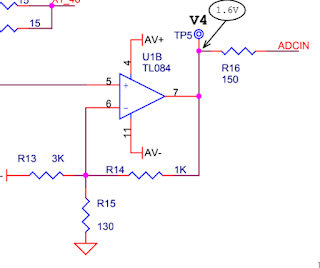
The root cause is the TL084. It is part of several stages in the input chain. It is powered by +-5V and if we look at the datasheet, the output voltage is capped depending on the power supply : With +-5v, the TL084 can actually only output about +-3V according to that spec The real value is much worse, it is actually VCC-4v to be safe (!) So only +-1 swing ! Raising the power supply is not an option, that would not be compatible with unmodified hardware Now let's compute the max value at every point of the input chain MAX @ G3 Max @ G2 Max @ G1B Max IN Max ADC G4 G3 G2 G1A G1G1B Friendly name Actual MAX IN SAT VALUE SAT ADC TL084 SAT V/DIV 1.50 8.00 0.1875 1.00 0.1875 2.00 0.09375 0.91 1.00 0.103125 20mv 20 2 1.50 8.00 0.1875 0.50 0.375 2.00 0.1875 0.91 1.00 0.20625 40mv 40 2 1.50 8.00 0.1875 0.25 0.75 2.00 0.375 0.91 1.00 0.4125 80mv 80 Max V/Div 2 1.50 8.00 0.1875 0.10 1.875 2.00 0.9375 0.91 1.00 1.03125 200mv 200 2 1.50 8.00 0.1875 0.05 3.

DSO 150 : Input Gain and not so good ADC accuracy

This is a follow up of 2 other posts about the dso 150 :  input gain  and  calibration While doing the fine calibration for the DSO, i noticed that on all ranges, the ADC swing was very low. It is a 12 bits ADC, so with one bit taken by the sign, it should leave 11 bits, i.e. +-2048 swing. I was seeing a much lower value, like 500 for the max value for a given range. So i went back to the input gain stages and computed the actual volt /div and the used volt/div The result is as follows : Real  Vanilla FW 20mv 5mv 40mv 10mv 80mv 20mv 200mv 50mV 400mv 100mV 800mv 200mV 2v 500mv 4v 1v 8v 2v 20v 5v 40v 10v 80v 20V (computed with 80% swing for each range, so we should be safe from the ADC point of view). As a result, we are only using 25% (1/4 = 2 bits)  of the ADC swing, so it acts as a 11-2=9 bits ADC. That explains why the accuracy is not that great.  So let's use the real swing value so that we have the full 11 bits accuracy whenever we can

DSO 150 : Calibration ? Nah, not really

Image
Both the official DSO firmwares and my own offer a "calibration". But actually, it is not a real calibration. It is a zero offset calibration. If we look at the schematic, we have several amplifying stages. The last stages is a bit special : It is also a shifting stage. Not only does it multiply the input by 1+1000/130 = 8.7, but it also shifts the input by +1.6 volt Why ? Because until now we were in AC mode, so the voltage could be in AV- / AV+ range (i.e ~ +-5V) After that last stage, we are in MCU mode, with a voltage between 0 and 3.3 v So,  the input is shifted by half of it (i.e. 3.3/2=1.6 v) to be able to sample negative AND positive voltages. -Vmax becomes zero, and +Vmax becomes 3.3v. We lose one bit of accuracy in the process to deal with the "sign". When you do a "calibration", you short circuit the inputs to get a zeo there and then the firmware reads what is the actual zero in the ADC, for each voltage range.

DSO 150, rotary encoder busted ? Simpler way to fix it

Image
A while back, i badly messed up the small PCB holding the rotary encoder and "fixed" it as described  here There is a simpler way to fix it : to not use the PCB at all. So even if it is full of short circuits, no problem. The gist of it is to bend the pins the OTHER way and to add extensions if needed. A picture is simpler than explaining it :

G600 Microscope Battery charging mod

Image
While thinking about replacing the mini usb connector to a micro one on my G600 microscope , i've  seen that   post  from Syonyk. Damn ! No real battery charging, straight to 5v. Warning : This is not an accurate analysis, it may contain errors or missing /misunderstood parts. Let's have a look. The partially reverse engineered/ contains error schematic /picture is as follows : The equivalent schematic is ( incomplete/may contain error ) : So indeed, VBUS (5v) is connected directly to VBAT through just a schottky (K14) and R12. On the other hand, the BMS circuit is tuned very low and will stop the charge at exactly 4.2 v. My battery is still healthy and only slightly puffy :) Let's use a real charging circuit and remove component so that VBUS is completely isolated from VBAT. Remove K14, the P-Mosfet (Q1) and R54 so that they are really isolated and there is no  resistor between VBUS and ground (R54). I also removed a very small cap/resistor

DSO 150 : Avoid 0.6v drop on power supply

Image
There is  a diode (D2)  acting as a reverse polarity protection circuit. It is very inefficient, we are loosing ~ 0.6 v there. Better to use a small SMD P-Mosfet transistor instead, such as A1SHB (cost ~ nothing) Voltage drop is now ~ 50 mV, much better, and we still have the reverse polarity protection

DSO150 : MCU fried ? No problem

Image
All of a sudden the board consumption jumped from 100 mA to 500 mA The regulator & MCU were getting REALLY hot After a bit of investigating, it appears that PD0 was shorted to ground INSIDE the MCU. It is most likely that  i've connected the analog board in the wrong pins and shorted it out. Ooops.... Now i'm really happy i've spent time watching  Louis Rossmann   entertaining videos :) No problem, let's take a bluepill board (2$ on ebay)  and swap the MCUs, they are both STM32F103 Hotair to remove the old & new ones , soldering iron, dragging solder THEN lot of flux to remove the shorts,  => No problem , back in business. The donor board The end result, with flux everywhere between the pins :) Thanks Louis ! The only issue i had to fix afterward was the MCU was running really really slow I had to resolder the C1 / C2 caps that are driving the quartz. Now everything is back to working state on my Frankenstein DSO 150, circa 2017.

DSO 150: Converting old analog board to new layout ( part 3 : remove Vbias )

Image
So now with have the ADC Bias driven by the -5v So let's remove VBIAS altogether, we dont need it and it will lower the consumption by a few mA I did it, and now coupling sel does not work anymore (AC/DC/GND selection) Wtf ? Ah, it so happens that VBIAS is used elsewhere :) Gotcha, it is the power supply for the AC/DC/GND switch. If we look at the new board layout, it is using 5v instead. The used pin is PA5. Let's check the pins : PA5 is not marked as 5v tolerant. Ok, let's check the new board layout again. Only protected by the 1k resistor. I guess that's ok, even if i dont like that much. So let's  remove R28, R22 and D1, connect left pad of D1 or R22 to AV+, and we are back All done on the analog board :)

DSO 150: Converting old analog board to new layout ( part 2: ADC Bias)

Image
Now we have to take care of the bias (VBIAS) For reference, that voltage is used to shift the voltage going to ADC by VCC/2=1.65 v It is done so that it can sample negative values. Without it you'd be only seeing positive voltage and all negative voltages would be stuck to ground. As said previously, the VBIAS was  causing a way for noise & temperature sensitivity to creep in. The old circuit was powering a 3v Zener from unregulated 8v input and using that as a voltage reference to shift the ADC voltage by ~ 1.65v . Since AV+ was ~ 8v, the R28 resistor was passing 5mA ((8v -3v)/1k), so that the zener was fully on. Now AV+ is only 5v, so the current is only 2mA, which is a bit low. The new board is using the regulated -5v as voltage reference to bias the last stage of the opAmp, like this : So the change is simple, remove R15 on the old board and replace it by a 3k resistor connected to -5v (AV-) The exact value you are looking for is 3030 Ohm,  3k +-