Posts

Showing posts from October, 2021

esp32C3: Using embedded jtag/usb to debug

Image
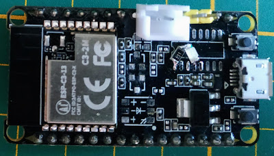
This is a follow up to the ESP32C3 jtag setup  The idea here is to detail the missing pieces in the documentation to use the embedded jtag/usb converter. I'll be a bit heavy handed in  removing stuff, it may not be 100% necessary. Your mileage may vary. Jtag setup The esp32c3 has regular jtag pins connected to GPIO 4/5/6/7 It also has a internal usb jtag+CDC/ACM connected to pins GPIO 18 & 19. By default it's using the usb/jtag one EFuse There is a efuse to automatically switch from internal jtag/usb to external jtag depending on the GPIO10 state at boot up It does not work , there is an   bug entry .  If you enable that bit (JTAG_SEL) it will use external jtag, period, never internal usb/jtag. Ifever you modified it, like i did, you can recover usb/jtag by setting the disable pad jtag efuse, and it will be locked on usb/jtag forever. In short, use USB/jtag only and dont play with the efuses. Leds everywhere On the devkit or similar boards from alibaba the jtag pins are als

DSO150/RiscV: Blaming the innocent

Image
While redoing the DSO150 on top of lnArduino i'm cleaning up a lot of stuff i just used  "as-is" previously. In particular, i rewrote the ILI9341 driver to be fast while still being portable to some extend. NB: It's a 8 bits parallel ILI9341 , not your vanilla SPI connected ILI9341. The new code worked fine on the GD32F303  (Arm) based unit but i ran into problems when used on the risc-v powered board (GD32VF103). Same DSO board, the two mcus have the  same hw components internally, just the core is different . I had strong doubt about the "lazy" write of the riscV chip.  If that happens, it means that when you write something, it is actually written a bit later. That's problematic when you are driving LCD signals. Adding fence/fence.i everywhere seemed to fix the obvious problem. But wait a sec,  adding  plain nops works also. So either delayed write issue or timing issue. Ok, we'll add the fence/nop and look into that later. Ah, the screen goes bla

DSO150+GD32VF103: Jtag strikes again

Image
 So after doing the small resistor removals, short, wiring  etc... we have now PB8 used in place of PB3  and PB3 is left unusued for the Jtag. The screen driver replaces on the fly  bit 3 by bit 8 when writing on the PB port.  After looking into it, it does not need to be optimised, as the code is using one or two colors at a time only. So the conversion is done once at the beginning of a sequence.  The speed loss is really small compared to vanilla code (like 0.5% slower). At worst we can compute a lookup table and lose 1kB of flash. Not worth it. Nice, let's display something and for ask the chip ID..... complete failure. And sometimes, i get a warning from openocd it has lost contact with the target. Bummer.  I  looked at my code, it looked completely correct.  I checked all the involved pins for bad soldering, all checked out ok. It took me a while to figure that one out (1 full day). It's the openocd message that gave me a hint.  The chip is configured by default to enable

DSO150 + longan nano chip / GD32VF103 ?

Image
 After upgrading a DSO shell with a GD303, let's upgrade one with a G32VF103 Why ? Why not. that chip is fast and has a FPU like the gd32f303. Additionnaly, it will be a good test bed for lnArduino, that works indifferently on those. While the GD32VF103 is more or less pin to pin compatible with the GD32F1 or STM32F1, there is one big difference : Arm chips are using SWD while the VF is using jtag.  We need 2 more pins : TDI (PA15) and TDO (PB3) On the DSO150, PA15 is used for the small red led. We dont need that. PB3 is more of a problem, it is used in the parallel display bus. So we'll have to use another B port pin and do on-the-fly bit swap. We'll use PB8, used for PWM comparator that is not used anyway. Let's go for the change : * Remove R8/R9: They are pull up/down resistors for SWD. No SWD, not needed. * Remove R14 to free up PA15 * Remove R43 to free up PB8 * Short circuit R35 to have a direct TDI signal to the MCU * Cut PB3 right next to the MCU and connect the