DSO150 + longan nano chip / GD32VF103 ?
After upgrading a DSO shell with a GD303, let's upgrade one with a G32VF103
Why ?
Why not. that chip is fast and has a FPU like the gd32f303. Additionnaly, it will be a good test bed for lnArduino, that works indifferently on those.
While the GD32VF103 is more or less pin to pin compatible with the GD32F1 or STM32F1, there is one big difference :
Arm chips are using SWD while the VF is using jtag.
We need 2 more pins : TDI (PA15) and TDO (PB3)
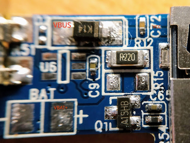
On the DSO150, PA15 is used for the small red led. We dont need that.
PB3 is more of a problem, it is used in the parallel display bus.
So we'll have to use another B port pin and do on-the-fly bit swap. We'll use PB8, used for PWM comparator that is not used anyway.
Let's go for the change :
* Remove R8/R9: They are pull up/down resistors for SWD. No SWD, not needed.
* Remove R14 to free up PA15
* Remove R43 to free up PB8
* Short circuit R35 to have a direct TDI signal to the MCU
* Cut PB3 right next to the MCU and connect the MCU PB3 to the jtag pin TDO
* Link the PB3 LCD pin to the left side of (removed) to the MCU PB8 (left pad of removed R43).
* Link PA15 to the Jtag TDI connector
* Link PB3 to the TDO pin of the connector
* Link PA13/SWD CLK to jtag TMS
* Link PA14/SWD IO to jtag TCK
Warning : The MCU pads are *very* fragile. If you heat them too much, the glue will come out and the pad will go.
The GD32VF103 shows up on openocd-riscv32, it's not completely dead. Success so far !

NB: The masking tape is to prevent the LCD from being scratched.

Comments
Post a Comment